- 您现在的位置:买卖IC网 > Sheet目录3872 > PIC18F4450T-I/ML (Microchip Technology)IC PIC MCU FLASH 8KX16 44QFN
239
XMEGA A [MANUAL]
8077I–AVR–11/2012
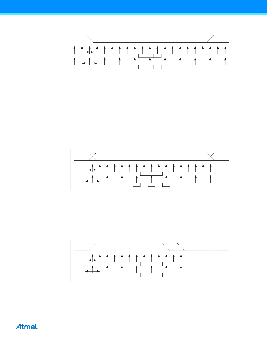
Figure 21-6. Start bit sampling.
When the clock recovery logic detects a high (idle) to low (start) transition on the RxD line, the start bit detection
sequence is initiated. Sample 1 denotes the first zero-sample, as shown in the figure. The clock recovery logic then uses
samples 8, 9, and 10 for normal mode and samples 4, 5, and 6 for double speed mode to decide if a valid start bit is
received. If two or three samples have a low level, the start bit is accepted. The clock recovery unit is synchronized, and
the data recovery can begin. If two or three samples have a high level, the start bit is rejected as a noise spike, and the
receiver looks for the next high-to-low transition. The process is repeated for each start bit.
21.8.2 Asynchronous Data Recovery
The data recovery unit uses sixteen samples in normal mode and eight samples in double speed mode for each bit.
Figure 21-7 on page 239 shows the sampling process of data and parity bits.
Figure 21-7. Sampling of data and parity bits.
As for start bit detection, an identical majority voting technique is used on the three center samples for deciding of the
logic level of the received bit. The process is repeated for each bit until a complete frame is received. It includes the first
stop bit, but excludes additional ones. If the sampled stop bit is a 0 value, the frame error (FERR) flag will be set.
Figure 21-8 on page 239 shows the sampling of the stop bit in relation to the earliest possible beginning of the next
frame's start bit.
Figure 21-8. Stop bit and next start bit sampling.
A new high-to-low transition indicating the start bit of a new frame can come right after the last of the bits used for
majority voting. For normal speed mode, the first low level sample can be at the point marked (A) in Stop Bit Sampling
and Next Start Bit Sampling. For double speed mode, the first low level must be delayed to point (B). Point (C) marks a
stop bit of full length at nominal baud rate. The early start bit detection influences the operational range of the receiver.
12
34
56
7
8
9
10
11
12
13
14
15
16
12
START
IDLE
0
BIT 0
3
123
4
5
678
12
0
RxD
Sample
(U2X = 0)
Sample
(U2X = 1)
12
34
56
7
8
9
10
11
12
13
14
15
16
1
BIT n
123
4
5
678
1
RxD
Sample
(CLK2X = 0)
Sample
(CLK2X = 1)
12
34
56
7
8
9
10
0/1
STOP 1
123
4
5
60/1
RxD
Sample
(CLK2X = 0)
Sample
(CLK2X = 1)
(A)
(B)
(C)
发布紧急采购,3分钟左右您将得到回复。
相关PDF资料
PIC18F4321T-I/ML
IC PIC MCU FLASH 4KX16 44QFN
PIC18F4221T-I/ML
IC PIC MCU FLASH 2KX16 44QFN
PIC18F2321T-I/ML
IC PIC MCU FLASH 4KX16 28QFN
PIC18F2221T-I/SO
IC PIC MCU FLASH 2KX16 28SOIC
PIC16LF1939-I/MV
IC MCU 8BIT 28KB FLASH 40-UQFN
PIC24F16KL402-I/SP
IC MCU 16BIT 16KB FLASH 28-SPDIP
PIC18F24J11-I/SS
IC PIC MCU FLASH 16K 2V 28-SSOP
PIC24F16KA101-I/SO
IC PIC MCU FLASH 16K 20-SOIC
相关代理商/技术参数
PIC18F4450T-I/PT
功能描述:8位微控制器 -MCU 16KB FL 768 RAM 34 I/O FS-USB 2.0 RoHS:否 制造商:Silicon Labs 核心:8051 处理器系列:C8051F39x 数据总线宽度:8 bit 最大时钟频率:50 MHz 程序存储器大小:16 KB 数据 RAM 大小:1 KB 片上 ADC:Yes 工作电源电压:1.8 V to 3.6 V 工作温度范围:- 40 C to + 105 C 封装 / 箱体:QFN-20 安装风格:SMD/SMT
PIC18F4455-BL
制造商:POWERLITE SYSTEMS 功能描述:PIC18F445 W/ BOOTLOADER FOR FLASHLAB 制造商:POWERLITE SYSTEMS 功能描述:PIC18F445 W/ BOOTLOADER, FOR FLASHLAB 制造商:POWERLITE SYSTEMS 功能描述:PIC18F445 W/ BOOTLOADER, FOR FLASHLAB; Silicon Manufacturer:Powerlite Systems; Core Architecture:PIC; Kit Contents:Board; Features:Bootloader Programming, RS232 Connector for Boot-Loading and Serial Comms ;RoHS Compliant: Yes
PIC18F4455-I/ML
功能描述:8位微控制器 -MCU 24kBF 2048RM FSUSB2 RoHS:否 制造商:Silicon Labs 核心:8051 处理器系列:C8051F39x 数据总线宽度:8 bit 最大时钟频率:50 MHz 程序存储器大小:16 KB 数据 RAM 大小:1 KB 片上 ADC:Yes 工作电源电压:1.8 V to 3.6 V 工作温度范围:- 40 C to + 105 C 封装 / 箱体:QFN-20 安装风格:SMD/SMT
PIC18F4455-I/P
功能描述:8位微控制器 -MCU 24kBF 2048RM FSUSB2 RoHS:否 制造商:Silicon Labs 核心:8051 处理器系列:C8051F39x 数据总线宽度:8 bit 最大时钟频率:50 MHz 程序存储器大小:16 KB 数据 RAM 大小:1 KB 片上 ADC:Yes 工作电源电压:1.8 V to 3.6 V 工作温度范围:- 40 C to + 105 C 封装 / 箱体:QFN-20 安装风格:SMD/SMT
PIC18F4455-I/PT
功能描述:8位微控制器 -MCU 24kBF 2048RM FSUSB2 RoHS:否 制造商:Silicon Labs 核心:8051 处理器系列:C8051F39x 数据总线宽度:8 bit 最大时钟频率:50 MHz 程序存储器大小:16 KB 数据 RAM 大小:1 KB 片上 ADC:Yes 工作电源电压:1.8 V to 3.6 V 工作温度范围:- 40 C to + 105 C 封装 / 箱体:QFN-20 安装风格:SMD/SMT
PIC18F4455T-I/ML
功能描述:8位微控制器 -MCU 24kBF 2048RM FSUSB2 RoHS:否 制造商:Silicon Labs 核心:8051 处理器系列:C8051F39x 数据总线宽度:8 bit 最大时钟频率:50 MHz 程序存储器大小:16 KB 数据 RAM 大小:1 KB 片上 ADC:Yes 工作电源电压:1.8 V to 3.6 V 工作温度范围:- 40 C to + 105 C 封装 / 箱体:QFN-20 安装风格:SMD/SMT
PIC18F4455T-I/PT
功能描述:8位微控制器 -MCU 24kBF 2048RM FSUSB2 RoHS:否 制造商:Silicon Labs 核心:8051 处理器系列:C8051F39x 数据总线宽度:8 bit 最大时钟频率:50 MHz 程序存储器大小:16 KB 数据 RAM 大小:1 KB 片上 ADC:Yes 工作电源电压:1.8 V to 3.6 V 工作温度范围:- 40 C to + 105 C 封装 / 箱体:QFN-20 安装风格:SMD/SMT
PIC18F4458-I/ML
功能描述:8位微控制器 -MCU 24KB Flash 2KB RAM RoHS:否 制造商:Silicon Labs 核心:8051 处理器系列:C8051F39x 数据总线宽度:8 bit 最大时钟频率:50 MHz 程序存储器大小:16 KB 数据 RAM 大小:1 KB 片上 ADC:Yes 工作电源电压:1.8 V to 3.6 V 工作温度范围:- 40 C to + 105 C 封装 / 箱体:QFN-20 安装风格:SMD/SMT